

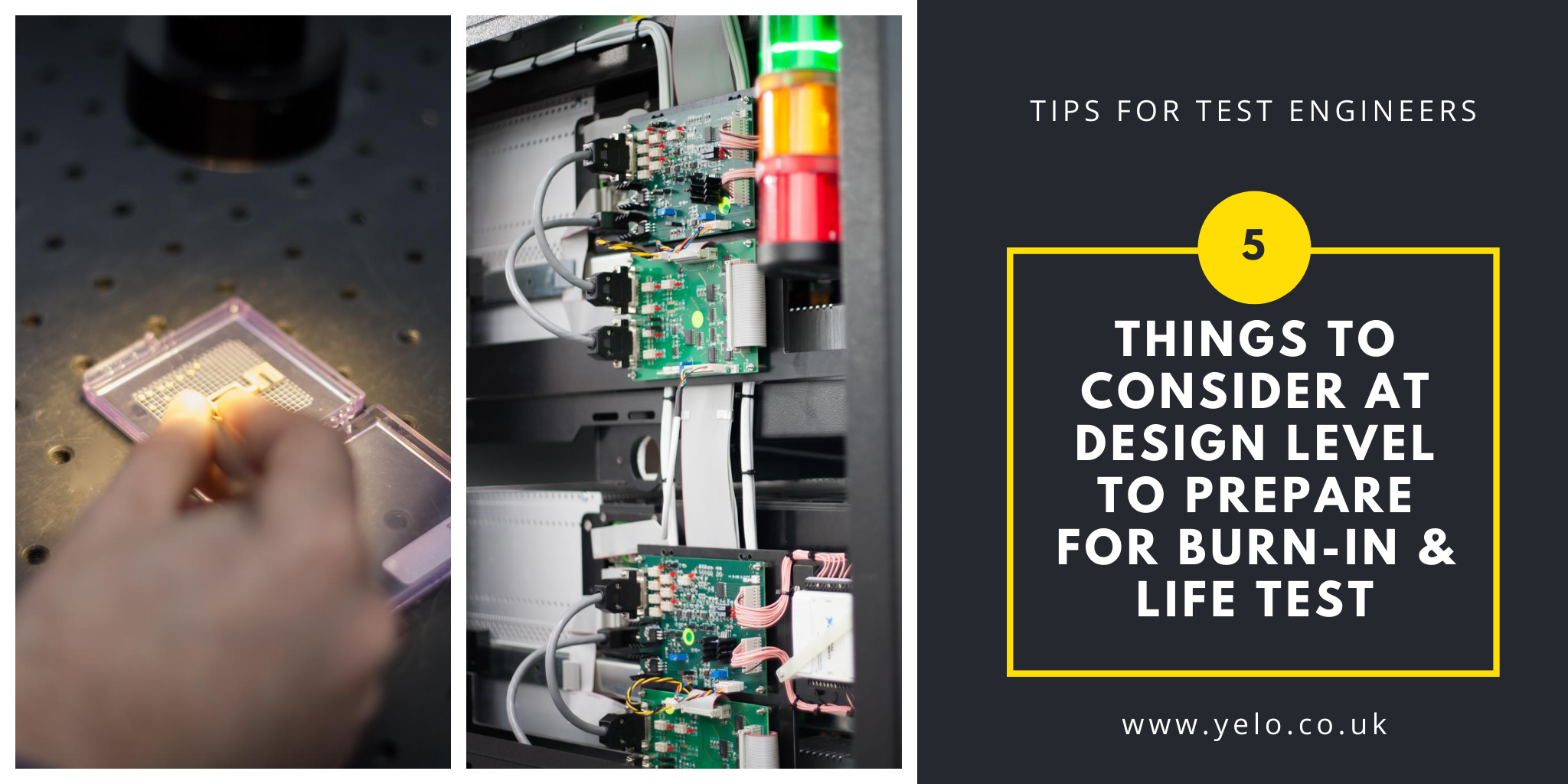

In the previous article we looked at some of the key failure mechanisms for laser diodes. In this article we aim to uncover some of the more technical and specific aspects of the device that need to be taken into consideration at design level.
There are 5 key considerations, technically, at design level.
• PAD Size
• PAD Location (wire bonding)
• Handling
• Material and Force
• Thermal Management
PAD size
The size of the PAD and current rating is going to determine what probing method is used.
PAD Location and wire bonding
It is critically important that want wire bonds are not in the vicinity of probes. It is very easy to snap damage a wire bond while probing and this will ultimately kill the device which can cause a premature failure.
Handling of device
It is important to consider how is the device is going to be handled in production environment.
Material and Force
When probing the device for burn-in, sufficient downward force is needed to make optimum thermal contact between the laser carrier and the burn-in heatsink. This presents a consideration for material e.g. Silicon can accept more force than Indium Phosphide.
Thermals
For burn-in, it is required to calculate power dissipation, surface area, material properties and flatness power per square mm as this will determine the temperature rise of the device. The parameters are the heat flow per square mm and the thermal resistance of the junction.
In our next article, we will look at a general overview of Burn-in.
