
A step by step outline on the production, test and burn-in of laser diodes and the challenges within this process.
Laser diodes have a wide range of uses, such as:
- Telecom and Datacom networks
- Analytical Instruments
- Barcode readers
- CD/DVD/blue ray disc reading and recording
- 3D printing
- LIDAR for building measurement and self0driving cars
- Medical instruments
The stages of the mass production of laser diodes are outlined below and is followed and explained in further detail:
- Wafer verification/fabrication
- Dicing/sawing
- Wire bonding to carrier
- COC test (Light Current Voltage, Wavelength Instruments)
- Burn-In
- Packaging
- Post package/final test
- Sell/ship
Throughout the production process it is essential that the yield at each stage ensures that: the test conditions are correct; the procedures are being followed; and the devices are of good quality. Testing accurately is a necessity within this process as there are numerous modes of failure for these devices, such as: infant mortality; the detection of poor wire bonding; and if the devices are of poor quality.
1. WAFER VERIFICATION/BUILDING
Modern laser diode device manufacturing begins with a round disc called a wafer. The wafer is created through the combination of gases mixed together in a MOCVD (metalorganic chemical vapour deposition) machine. This is a chemical vapour deposition method used to grow crystalline layers to create complex semiconductor multilayer structures.
The MOCVD machine mixes the following gases:
▪ Indium Phosphide (InP)
▪ Indium gallium phosphide (InGaP)
▪ Indium gallium arsenide (InGaAs)
▪ Gallium Arsenide GaAs
Why are these gases used?
Semiconductor devices and circuits employs III–V technology, because it is based on crystalline compounds formed by combining metallic elements from column III and non metallic elements from column V of the periodic table of chemical elements.
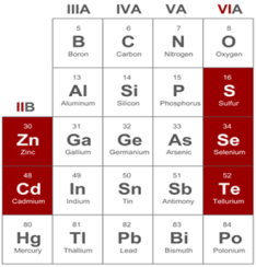
The most commonly used semiconductor materials are crystalline inorganic solids. These materials are classified according to the periodic table groups of their constituent atoms.
However, costs can occur during the wafer manufacturing stage. Hard costs such as the loss of gases through the transformation into energy and the time scale of making the wafer can be lost during the process, if any mistakes or problems occur.
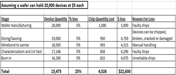
During the stage, there is usually an average of a 5% loss or damage of chips. (Please see table outlining costs and losses)
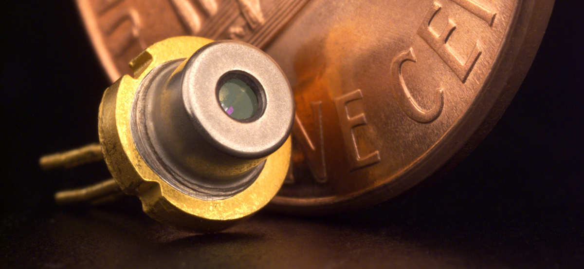
2. DICING/SAWING
Once the wafer has been fully manufactured it is necessary that the wafer is diced up into individual die so that light can be emitted through the broken edge of the material.
During the dicing process some devices maybe lost, damaged, broken or cracked. This results in a loss of both opportunity costs and materials.
The process is outlined below:
- Die are separated from the semi conductor wafer
- The dicing process can be carried out by scribing and breaking the wafer using mechanical sawing or laser cutting
- During dicing, wafers are typically mounted to dicing tape which has a sticky backing that holds the wafer onto a thin metal sheet
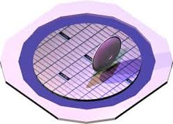
Below is an image of a wafer being diced by a saw:
3. WIRE BOND TO CARRIER
Wire bonding is the process of making inter connections between the semiconductor wafer and its packaging. It is considered to be the most cost-effective and flexible method of interconnection technology. It is used to assemble the vast majority of semiconductor packages.
There are numerous types of packaging that can be used in laser diode manufacturing, such as:
- TO-can
- Minidil
- Butterfly
- CoC
- TOSA
4. LASER DEVICE CHARACTERISATION TEST - LIV TEST
Once the devices have been bonded to their carriers their performance characteristics will be analysed, such as optical power, spectrum, near field and far field measurements, in a characterization test.
The devices will also be LIV tested, which is an essential test that a laser diode must go through to ensure its reliability for post production use. It will help to verify the operating characteristics of the devices by driving current to the laser diodes and measuring the resulting voltage and light output.
During this stage an estimated 5% of the devices can be lost through: handling; dropping chips from tweezers; scratching/damaging chips and losing chips.
5. BURN-IN
Burn-In tests are applied to laser diodes during the manufacturing process. This is a necessary step as it identifies any potentially defective devices and is used to screen out lasers with short life expectancies. During this stage, around 5% of the remaining diodes will be lost due to the identification of defective or unreliable chips.
6. PACKAGING
Once the devices have been tested thoroughly they will be placed into their appropriate packaging. i.e. added into an integrated circuit or a TO-can package.
7. POST PACKAGE/FINAL TEST
Devices are tested for a final time to confirm that the chips demanded by customers are reliable and perform effectively.
8. SELL/SHIP
Laser diodes are sent out to customers.
Below is a table outlining the costs at each stage of the production process and what losses have occurred.